
Intel Foveros Direct: Revolutionizing Advanced Packaging Technology
Monday, December 02, 2024Intel Foveros Direct: Revolutionizing Advanced Packaging Technology

Intel's Foveros Direct is a cutting-edge packaging technology set to revolutionize the semiconductor industry. This innovative approach allows for more flexible and tighter integration between chiplets, resulting in lower latency, higher bandwidth, and reduced die area required for communication. Let's dive into the details of Intel Foveros Direct, its key features, and its potential impact on the tech world.
Understanding Foveros Direct
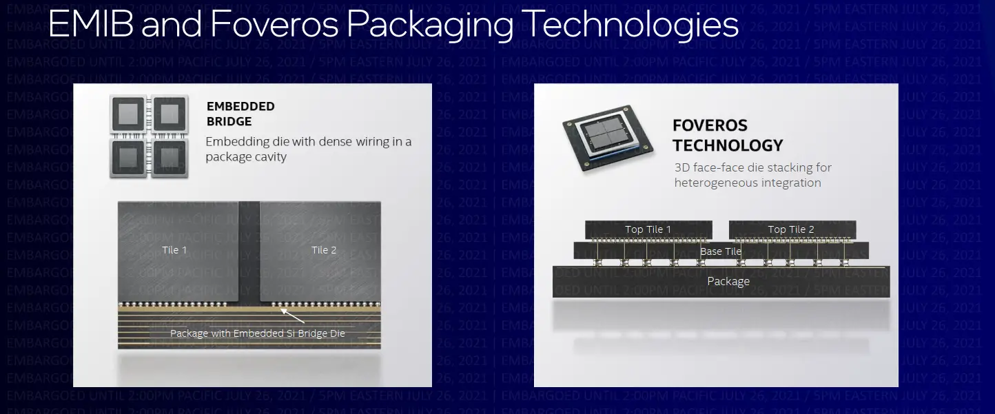
Foveros Direct is Intel's next-generation advanced packaging technology that enables direct copper-to-copper connections between chiplets. Unlike traditional solder connections, which can slow down data transfer, Foveros Direct uses direct copper-to-copper connections, resulting in lower latency and higher bandwidth. This technology allows for more efficient communication between different components of a chip, making it ideal for high-performance applications.
Key Features of Foveros Direct
Direct Copper-to-Copper Connections: By utilizing direct copper-to-copper connections instead of traditional solder connections, Foveros Direct achieves lower latency and higher bandwidth.
Reduced Die Area: This approach reduces the die area required for communication between chiplets, allowing for more compact and efficient chip designs.
Enhanced Performance: Improved communication between chiplets leads to enhanced overall performance, making Foveros Direct ideal for high-performance applications such as gaming, data centers, and artificial intelligence.
Scalability: Foveros Direct is scalable and can be used for a wide range of applications, from low-power devices to high-performance computing systems.
How Foveros Direct Works
Foveros Direct works by thermocompression bonding of copper vias on individual chiplets to those on a wafer or even direct bonding of entire wafers stacked atop each other. This process allows for the creation of complex system modules with improved performance and efficiency. The technology blurs the boundary between the end of the wafer and the beginning of the package, resulting in a seamless integration of different components.
Potential Applications of Foveros Direct
Gaming: Foveros Direct can significantly improve the performance of gaming GPUs by enabling faster data transfer and more efficient communication between different components.
Data Centers: The technology can enhance the performance and efficiency of data center processors, making them more suitable for handling large-scale computing tasks.
Artificial Intelligence: Foveros Direct can improve the performance of AI accelerators, enabling faster processing of complex algorithms and data analysis.
Consumer Electronics: The technology can be applied to consumer electronics such as smartphones and tablets, resulting in more powerful and energy-efficient devices.
Impact on the Semiconductor Industry
The introduction of Foveros Direct is expected to have a significant impact on the semiconductor industry. By enabling more efficient communication between chiplets, the technology can lead to the development of more powerful and energy-efficient chips. This, in turn, can drive innovation in various sectors, from consumer electronics to data centers and artificial intelligence.
Conclusion
Intel's Foveros Direct is a groundbreaking advanced packaging technology that promises to revolutionize the semiconductor industry. With its direct copper-to-copper connections, reduced die area, and enhanced performance, Foveros Direct is set to become a key player in the development of high-performance chips. As the technology continues to evolve, it will likely have a profound impact on various industries, driving innovation and improving the efficiency of electronic devices.