
Intel 18A Yields in 2025: Unpacking the 10% Controversy, Progress, and Future Outlook
Monday, February 24, 2025Intel 18A Yields in 2025: Unpacking the 10% Controversy, Progress, and Future Outlook
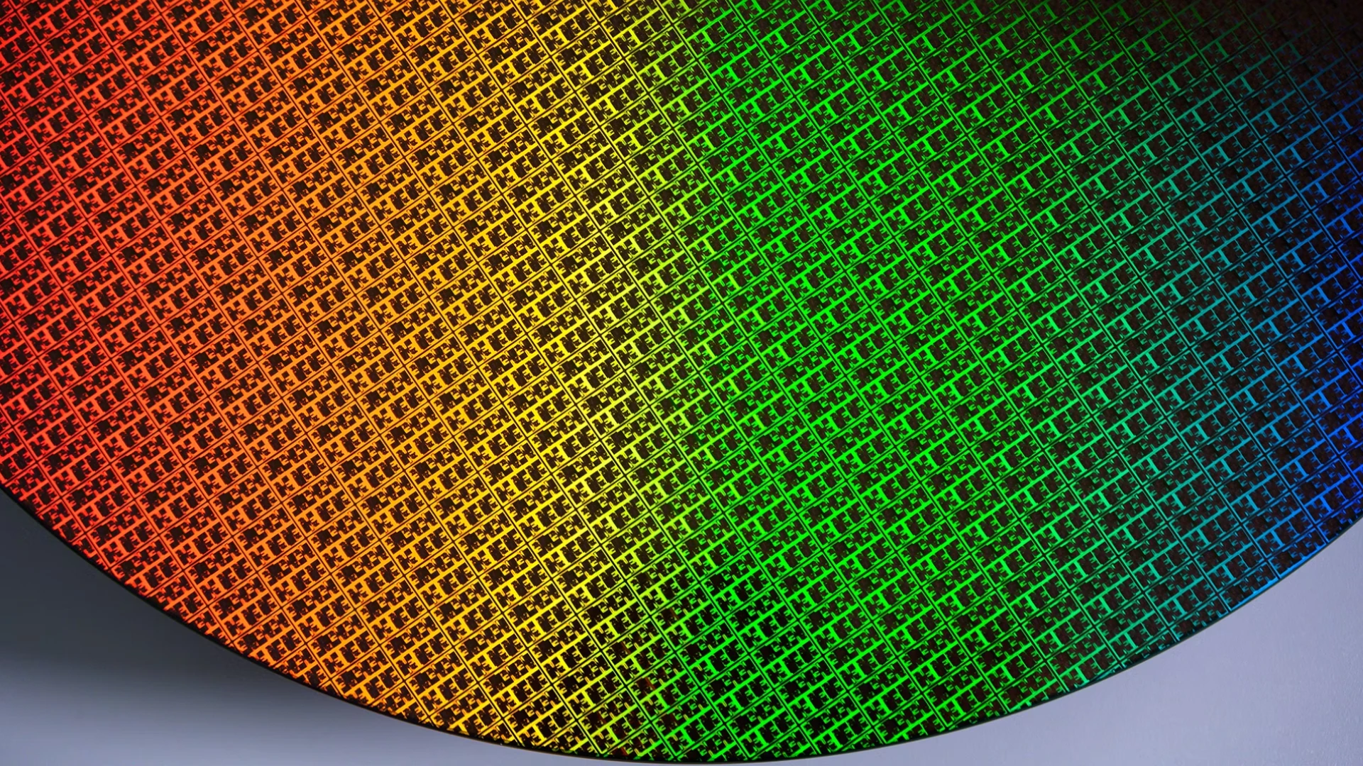
The semiconductor industry, a realm of relentless innovation and fierce competition, finds itself at a pivotal juncture as of February 24, 2025, with Intel’s 18A process node sparking widespread discussion and debate. This advanced manufacturing technology, representing the culmination of Intel’s ambitious "5 Nodes in 4 Years" roadmap, has become a lightning rod for speculation, particularly regarding its production yields. Yields—the percentage of functional chips harvested from a silicon wafer—are the lifeblood of cost efficiency and scalability in chipmaking, and Intel’s 18A node, poised to power next-generation processors for the AI-driven era, is no exception. Reports of dismal yields as low as 10% have clashed with Intel’s optimistic updates, creating a narrative rich with technical nuance, industry stakes, and competitive intrigue. This article delves deeply into the state of Intel 18A yields, weaving together official statements, technical analyses, industry context, and forward-looking projections to offer a thorough exploration of where this critical technology stands today.
The Genesis and Promise of Intel 18A
To fully appreciate the yield controversy surrounding Intel 18A, one must first understand its significance within Intel’s broader strategic vision. Launched as part of a bold plan unveiled by former CEO Pat Gelsinger, the "5 Nodes in 4 Years" initiative aimed to catapult Intel back to the forefront of semiconductor manufacturing after years of challenges with its 10nm and 7nm nodes. Intel 18A, shorthand for 1.8 nanometers (though modern node names are more marketing than literal measurements), marks the fifth and final step in this accelerated roadmap, following Intel 7, Intel 4, Intel 3, and Intel 20A. Scheduled for production in 2025, with a high-volume ramp-up anticipated in 2026, 18A is not merely an incremental improvement but a technological leap, incorporating two groundbreaking innovations: RibbonFET and PowerVia.
RibbonFET, Intel’s branding for Gate-All-Around (GAA) transistors, replaces the traditional FinFET design with a more efficient structure that wraps the gate around the transistor channel on all sides, enhancing control over current flow and boosting performance while reducing leakage. PowerVia, meanwhile, introduces backside power delivery, a novel approach that separates power lines from signal interconnects by routing power through the back of the wafer. This architectural shift promises up to 15% better performance per watt and a remarkable 30% increase in chip density compared to the Intel 3 node, according to Intel’s own specifications (Intel 18A Process). These advancements position 18A as a cornerstone of Intel’s foundry ambitions, targeting both its own products—like the Panther Lake client processor and Clearwater Forest server CPU—and external customers seeking cutting-edge silicon for AI workloads.
The Yield Conundrum: What Are We Measuring?
At the heart of semiconductor manufacturing lies the concept of yield, a metric that determines the viability of a process node. Yield is defined as the proportion of defect-free chips produced from a wafer, expressed as a percentage. For mature nodes like TSMC’s 7nm or Intel’s Intel 7, yields often exceed 80-90%, reflecting years of refinement. However, new nodes, especially those pushing the boundaries of physics at sub-2nm scales, typically start with lower yields—sometimes as low as 20-30%—before optimization drives them higher. Yield depends on several factors: defect density (the number of defects per square centimeter), die size (larger chips are more prone to defects), and the maturity of the manufacturing process. A low yield translates to higher costs, as more wafers must be processed to produce a given number of functional chips, making it a critical hurdle for Intel 18A’s success.
The controversy erupted when South Korean outlet Chosun Daily published a report claiming Intel 18A yields were languishing at a mere 10%, a figure that, if true, would render mass production economically unfeasible (Intel 18A Yields Report). This bombshell reverberated across the tech world, amplified by rumors that Broadcom, a potential foundry customer, had tested 18A and canceled orders, deeming it unprepared for high-volume manufacturing (HotHardware Report). Such a yield would place Intel 18A in stark contrast to competitors like TSMC, whose N3E (3nm Enhanced) process reportedly achieves yields of 84-90%, or even Samsung, which struggled with sub-20% yields on its second-gen 3nm node (TrendForce News). But is this 10% figure a fair representation of Intel’s progress, or a distortion of a more complex reality?
Dissecting the 10% Yield Claim
The 10% yield report has faced significant pushback, both from Intel and independent analysts, who argue it lacks context and specificity. Semiconductor yields are not a one-size-fits-all metric; they vary dramatically depending on the size of the chip being produced. A defect density—the average number of manufacturing flaws per unit area—determines how many dies on a wafer are affected. Larger dies, such as those used in high-end server CPUs or GPUs, are more likely to encounter a defect, reducing their yield, while smaller dies, like those in chiplet-based designs, fare better. TechPowerUp, a respected hardware analysis site, crunched the numbers using a defect density of 0.4 defects per cm²—a figure Intel reportedly achieved by August 2024—and various yield models to illustrate this variability (TechPowerUp Yield Analysis).
For a massive 858 mm² die, akin to a monolithic server chip, the Poisson yield model predicts a dismal 3.23%, while Murphy’s model yields 7.95%—numbers that could plausibly align with the 10% rumor if rounded or misreported. However, for smaller dies like Panther Lake’s CPU+NPU tile (114.304 mm²), yields jump to 44.5% (Poisson) or 64.4% (Murphy), and for an even smaller GPU tile (53.6 mm²), they reach 81.0% (Poisson) or 86.5% (Murphy). These calculations suggest that the 10% figure might reflect yields for a specific, large test chip—perhaps one Broadcom evaluated—rather than the process as a whole. Intel’s increasing reliance on chiplet architectures, where processors are built from smaller, modular tiles connected via technologies like Foveros and EMIB, further supports the idea that practical yields for production chips could be significantly higher.
Intel’s Response and Tangible Progress
Intel has staunchly refuted the 10% yield narrative, though it has not released precise figures—a standard practice to safeguard competitive secrets. In September 2024, the company announced a major milestone: the 18A process was "powered on, healthy, and yielding well," with Panther Lake and Clearwater Forest chips fabricated, booted, and running operating systems (SiliconANGLE Update). This achievement, detailed by Intel VP Kevin O’Buckley, underscored that the process had moved beyond theoretical development into tangible results, with customer tape-outs scheduled for the first half of 2025 and production ramp-up planned for 2026 (Intel 18A Progress).
Pat Gelsinger, shortly after stepping down as CEO, took to X to dismiss the Chosun Daily report, declaring, “I am very proud of the 18A team and their work,” and hinting at misinformation in the yield rumors (Pat Gelsinger X Post). Industry analyst Ben Bajarin, interpreting Gelsinger’s earlier confidence—where he once said he’d “bet the company” on 18A—suggested yields might be closer to 60%, consistent with a defect density below 0.4 (PC Gamer Analysis). These statements paint a picture of a process overcoming early hurdles, aligning with Intel’s timeline despite external skepticism.
Technical Nuances and Yield Modeling
To further unpack Intel 18A’s yield potential, consider the mathematical models used in the industry: Poisson, Murphy, Exponential, and Seeds. Each offers a different lens on yield based on defect density and die area. The Poisson model, the simplest, assumes defects are randomly distributed and calculates yield as , where is die area and is defect density. Murphy’s model, more conservative, squares this probability, while Seeds adjusts for clustering. For a defect density of 0.4 defects per cm², the results are telling:
Y = e^{-A \cdot D}AD- Large Die (858 mm²): Poisson = 3.23%, Murphy = 7.95%, Seeds = 22.56%
- Panther Lake CPU+NPU (114.304 mm²): Poisson = 44.5%, Murphy = 64.4%, Seeds = 67.8%
- Panther Lake GPU (53.6 mm²): Poisson = 81.0%, Murphy = 86.5%, Seeds = 90.2%
These figures, derived from TechPowerUp’s analysis, highlight a critical advantage of Intel’s chiplet strategy: smaller dies dramatically improve yields, potentially offsetting challenges with larger test structures. Moreover, Intel’s adoption of backside power delivery (PowerVia) could reduce defect risks in interconnect layers, while RibbonFET’s GAA design may enhance transistor reliability—factors that might not yet be fully reflected in early yield data (IEEE Spectrum Insight).
The Competitive Landscape
Intel 18A does not exist in a vacuum; its yields must be benchmarked against rivals. TSMC’s N3E, a 3nm-class node, reportedly achieves 84-90% yields, underpinning its dominance in high-performance computing and mobile chips. Samsung, meanwhile, has grappled with its 3nm GAA process, with yields below 20% delaying mass production—a reminder that advanced nodes universally face teething problems. Intel’s unique combination of RibbonFET and PowerVia offers a differentiator, potentially delivering superior power efficiency and density, but only if yields reach competitive levels (Intel 18A Technical Insights). The stakes are high, as TSMC’s upcoming N2 (2nm) node looms on the horizon, intensifying pressure on Intel to prove 18A’s foundry credentials.
Looking Ahead: Challenges and Optimism
As of February 24, 2025, Intel 18A stands at a crossroads. The 10% yield rumor, while alarming, appears to be an oversimplification, likely tied to specific large-die tests rather than the process’s broader capability. Intel’s milestones—functional Panther Lake and Clearwater Forest chips, a defect density trending below 0.4, and a clear production timeline—suggest a trajectory toward viability. The company’s chiplet approach, leveraging smaller, higher-yielding dies, aligns with modern design trends, potentially mitigating early yield concerns. Yet challenges remain: refining defect density further, scaling to high-volume production, and convincing foundry customers like Broadcom of 18A’s readiness.
The road ahead is fraught with technical and market hurdles, but Intel’s progress offers cause for cautious optimism. By mid-2025, customer tape-outs will provide a clearer picture, and by 2026, the ramp-up to high-volume manufacturing will test 18A’s mettle. For now, the evidence leans toward Intel overcoming initial obstacles, positioning 18A as a contender in the AI computing revolution—and a testament to the resilience of a company determined to reclaim its silicon crown.