
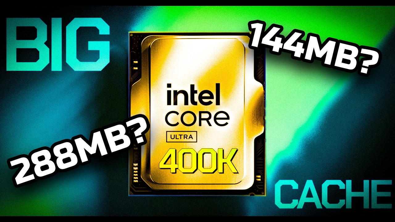
Intel Nova Lake bLLC: 288MB Cache vs AMD 9950X3D2 Detailed
Monday, April 20, 2026Intel Nova Lake bLLC Cache Fully Mapped: 288MB Flagship, New 400D and 400DX Branding, and a Direct Shot at AMD's 9950X3D2
The cache picture for Intel's Nova Lake-S desktop lineup is now substantially clearer. A new pair of posts from hardware leaker Jaykihn has filled in the specific cache totals for every bLLC-equipped SKU in the Core Ultra 400 family, confirmed that bLLC parts will carry distinct 400D (single-tile) and 400DX (dual-tile) branding, and revealed how the cache is physically structured inside each compute tile. Taken alongside a Wccftech analysis comparing the numbers to AMD's just-launched Ryzen 9 9950X3D2, the data puts Intel's most cache-heavy parts at 38% more total L3 cache than AMD's current dual-3D V-Cache flagship.
None of this is officially confirmed by Intel. These are pre-release leaks from a well-sourced tipster, and the specifications will evolve before Nova Lake ships — currently expected at CES 2027 for desktop parts. But the level of detail now available gives a clearer picture of what Intel is actually building to compete for the gaming CPU crown, and it is more aggressive than many expected.
The Five bLLC Cache Tiers: From 108MB to 288MB
Jaykihn's most recent post lists five specific cache totals mapped to their core configurations, covering both single-tile and dual-tile variants. The full breakdown of bLLC-equipped SKUs is as follows:
- 16P + 32E (dual tile) → 288MB — The flagship 52-core configuration with two full compute tiles
- 16P + 24E (dual tile) → 264MB — The 44-core dual-tile SKU with one tile at full P-core count and the other with 8P + 12E
- 8P + 16E (single tile) → 144MB — The 28-core single-tile "Premium Gaming" configuration
- 8P + 12E (single tile) → 132MB — A 24-core single-tile variant
- 6P + 12E (single tile) → 108MB — An entry bLLC tier with a non-K 65W configuration
The five-tier cache structure is important because earlier leaks had established that bLLC would exist but had left the specific cache totals for the 44-core and multi-variant single-tile parts as open questions. The previous framing of "up to 288MB" was accurate for the flagship but did not explain how Intel would scale the feature across the lineup. These new numbers answer that question: the cache scales predictably with core count and compute tile size, with 144MB per full bLLC compute tile across all configurations.
How the Cache Is Built: Intel's 12MB Slice Architecture
The second of Jaykihn's posts adds structural detail on how those totals are assembled inside the chip. The bLLC cache is organized around 12MB slices, with the allocation tied directly to the core clusters. One P-core cluster carries two shared 12MB slices of L3 cache. One E-core cluster carries one 12MB slice. Jaykihn described the formula as "4×(2×12) + 3×12" for the standard bLLC single-tile — which on the 8P + 16E configuration resolves to 96MB from P clusters plus 48MB from E clusters, totalling 144MB per tile.
For non-bLLC standard Nova Lake chips, the slice size is 3MB per cluster rather than 12MB, keeping total L3 in the 36MB range for a standard 8+16 die — consistent with what modern Arrow Lake parts carry. The bLLC version effectively quadruples the per-cluster cache allocation, which is what makes the 144MB-per-tile figure possible without physically stacking additional SRAM dies on top of the cores.
This architectural difference from AMD's approach is significant and worth examining in detail.
bLLC vs AMD 3D V-Cache: Two Different Philosophies
AMD's 3D V-Cache technology works by vertically stacking additional SRAM dies on top of the CPU's core dies using Through-Silicon Via (TSV) bonding — a process that is physically complex and thermally challenging, since the stacked cache layer sits between the cores and the IHS, affecting heat dissipation. AMD's second-generation 3D V-Cache in the Ryzen 9000X3D series places the cache below the CCD rather than above it, addressing the worst thermal issues while maintaining the stacking approach.
Intel's bLLC does not stack additional dies. The cache is integrated directly into the compute tile's silicon — it is an on-die expansion of the last-level cache rather than a physically separate SRAM package bonded onto the chip. This means no additional bonding complexity, no thermal interference from a stacked die, and potentially more predictable access latency since the cache is on the same silicon layer as the cores. The trade-off is die size: the bLLC compute tile grows from 98mm² (standard) to 154mm² (bLLC), a 57% increase in die area to accommodate the larger on-die cache. That larger die translates to higher manufacturing cost per tile and will be reflected in premium pricing for D and DX series SKUs.
There is also a structural advantage Intel claims in how bLLC scales across multi-tile designs. AMD's current X3D implementation places the V-Cache on only one CCD in multi-CCD processors, creating cache asymmetry — cores on the non-X3D CCD have dramatically less L3 cache than cores on the X3D CCD. Windows task schedulers and game engines must account for this asymmetry by preferring to schedule threads on the X3D CCD, and they do not always succeed in doing so optimally. Intel's approach places 144MB of bLLC on each compute tile symmetrically, so all cores in a dual-tile Nova Lake CPU — whether on tile one or tile two — have equal access to their local 144MB pool. This symmetric layout eliminates the scheduling problem AMD has faced with multi-CCD X3D designs, though inter-tile cache access on a dual-tile CPU still introduces latency when one tile needs data from the other tile's cache.
The D and DX Branding: Intel's Return to HEDT Segmentation
The 400D and 400DX naming convention represents Intel formalizing a new tier within the Core Ultra 400 lineup to distinguish bLLC-equipped parts from standard SKUs. The naming follows a logic similar to AMD's "X3D" suffix: a standard chip with the same core count gets a different designation when it carries the large cache. The D suffix marks single-tile bLLC parts — those carrying 108MB, 132MB, or 144MB of cache. The DX suffix marks dual-tile bLLC parts — the 264MB and 288MB configurations.
The DX tier in particular resurrects an HEDT-adjacent product concept. Intel discontinued its Core-X HEDT line years ago, leaving workstation users without a consumer option between mainstream desktop CPUs and full Xeon server parts. The dual-tile Nova Lake DX chips — 44 cores at 264MB or 52 cores at 288MB — serve a function similar to the old Core-X platform: more cores, more cache, higher power delivery requirements than standard consumer boards can handle, and a premium price that places them above the mainstream lineup. Whether Intel markets them under a separate "Core Ultra X" branding (as has been speculated) or integrates them into the Core Ultra 400 family with just the DX designation remains unconfirmed.
There is also a locked (non-K) 65W bLLC variant in the mix — a 6P + 12E + 4 LPE configuration with 108MB of cache. This part sits outside the D/DX branding system, described by Jaykihn as a model "being moved around depending on how it comes to market." The existence of a power-efficient bLLC part suggests Intel is considering making the cache feature available to small form factor and low-power desktop builds, not just the high-TDP enthusiast segment.
The AMD 9950X3D2 Comparison: 38% More Cache on Paper
AMD launched its Ryzen 9 9950X3D2 Dual Edition on April 22, 2026 at a retail price of $899. The chip carries 16 Zen 5 cores with dual 3D V-Cache, bringing total L3 cache to 192MB and total cache (L2 + L3) to 208MB. It is AMD's most cache-dense consumer desktop processor to date, doubling the V-Cache of the original 9950X3D by stacking two V-Cache dies rather than one.
Comparing Intel's Nova Lake bLLC figures to this specific reference point:
- The 264MB dual-tile Nova Lake DX part carries 27% more total cache than AMD's 9950X3D2
- The 288MB flagship dual-tile DX part carries 38% more total cache than AMD's 9950X3D2
- Even the 144MB single-tile Nova Lake D part carries about 38% less cache than the 9950X3D2, but more than the single-tile 9950X3D at 128MB total cache
These raw cache count comparisons have real performance implications — but also real limits. The relationship between cache size and gaming performance is not linear. AMD's 3D V-Cache gains documented in real benchmarks typically range from 5% to 30% in cache-sensitive titles, with some games benefiting substantially and others seeing minimal uplift. Cache is most beneficial when the working set of game data fits within the expanded cache, allowing the CPU to avoid costly round-trips to DRAM. Beyond the saturation point where even larger caches do not fit significantly more useful data, the gains plateau.
Whether Intel's 288MB of on-die bLLC translates to gaming performance proportional to the cache count advantage over AMD's 208MB is unknown until actual benchmarks ship with Nova Lake hardware. Intel's internally projected bLLC gaming uplift over Arrow Lake is 30–45%, which is competitive with or exceeds AMD's 3D V-Cache gains over non-X3D AMD equivalents. But projections from the manufacturer's own pre-release documents carry the obvious caveat that they represent best-case scenarios.
How Many Nova Lake SKUs Get bLLC?
An important constraint in the Nova Lake bLLC story is the limited distribution of the feature across the full 12-SKU Nova Lake desktop lineup. Only three to five SKUs are confirmed to receive bLLC across all configurations — the three primary D and DX parts plus potentially the 65W non-D locked variant. The remaining seven to nine SKUs in the lineup use standard compute tiles with 36MB of L3 cache, keeping them directly comparable to current-generation desktops in cache terms.
This contrasts with AMD's approach, which has offered 3D V-Cache across a broader price range of Ryzen X3D chips. The Ryzen 7 9800X3D at around $479 is AMD's most popular X3D gaming CPU and delivers the core V-Cache gaming gains at a sub-$500 price point. AMD has made the cache feature accessible well below the flagship tier. Intel's bLLC, based on current leak information, appears concentrated in the upper tiers of the Nova Lake lineup — the D and DX parts will command significant price premiums given the larger die area required.
The broader availability picture will become clearer as Nova Lake's pricing is officially revealed. The 65W non-K bLLC part hints at Intel considering wider distribution, but until the full pricing ladder is confirmed, it is reasonable to expect bLLC Nova Lake parts to be priced in the $400–$900+ range, mirroring the premium that X3D parts carry over their non-X3D equivalents.
Shared L2 Cache: Another Nova Lake Architecture Change
Alongside the bLLC details, Jaykihn has separately noted that Nova Lake introduces a shared L2 cache design, replacing the private per-core L2 caches that Intel has used for 17 years. In current Intel CPU designs, each physical core has its own dedicated L2 cache. Nova Lake moves to a shared model where L2 cache is pooled across clusters of cores rather than allocated exclusively to individual cores.
Shared L2 cache designs can improve L2 utilization efficiency — cores that are not working hard do not hold L2 capacity reserved but unused, while heavily loaded cores can draw from a larger shared pool. The trade-off is potential contention between cores sharing an L2 pool when multiple cores are simultaneously demanding cache access. Whether Nova Lake's shared L2 implementation favors the efficiency gains or introduces contention penalties in heavy multi-threaded workloads is an empirical question that only real-hardware benchmarks will answer.
The Gaming Cache War Is Just Getting Started
What is clear from the Nova Lake bLLC leak is that the desktop CPU market is entering an era of aggressive cache competition that will extend well beyond the current generation. AMD is reportedly developing Zen 6 X3D variants that may carry up to 240MB of 3D V-Cache — which would partially close the gap with Nova Lake's 288MB flagship DX chip while competing on the architectural improvements Zen 6 brings to core performance. Intel's bLLC approach, by integrating the cache into the silicon itself rather than stacking it externally, gives the company more flexibility in scaling and potentially reduces some of the manufacturing complexity constraints that limit AMD's V-Cache quantities per die.
The fundamental dynamic is straightforward: after years of AMD owning the gaming CPU segment through 3D V-Cache while Intel had no cache-competitive response, Nova Lake with bLLC is Intel's first serious attempt to fight on that specific battlefield. The specifications suggest Intel has gone large — potentially too large for the cache to show proportional real-world gains in most gaming titles, but certainly large enough to ensure the company is not outclassed on a benchmark sheet. The actual gaming performance of these chips, and where AMD lands with Zen 6 X3D in response, will determine who wins the next round. That fight should arrive in force around CES 2027.
Want more Intel Nova Lake coverage, AMD Ryzen X3D analysis, and desktop CPU news? Browse our other posts for the latest on Nova Lake specs, bLLC, and next-generation gaming CPU performance.