
Intel's 18A Cells Are 30% Taller Than a Node Samsung Shipped Years Ago. The Teardown Says So
Monday, September 28, 2026By Indie Kings | September 28, 2026
Updated September 28, 2026: SemiAnalysis has published a free teardown of Intel Panther Lake, and it is the first actual measurement of 18A rather than another roadmap claim. The headline is not the one the marketing implies. Intel's 18A P-core cells measure 550 nm high-fin-width against Samsung's 423 nm on SF2, a node Samsung shipped in GAA form years earlier, and 18A logic is a five-track library where Intel's own Intel 3 and TSMC's N3E are both seven-track. Measured in the same representative-cell model the lab uses for density, 18A compute logic and TSMC N3E come out similar, with the 18A example 18.6 percent denser than Intel 3's GPU tile. The other half of the story is where Intel won outright: moving power to the back of the wafer freed frontside routing, and the 18A P-core's lowest metal layer has 2.63 times the cross-sectional area of the N3E vector engine, 1.84 times after normalising for pitch.
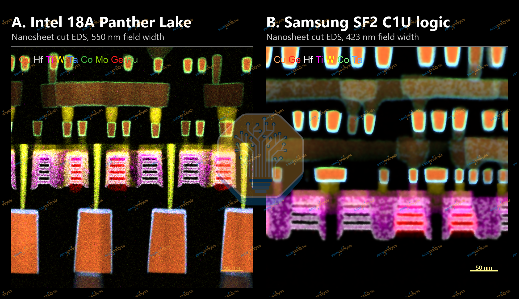
Image: Intel 18A P-core logic beside Samsung SF2 logic, showing Intel's larger cell footprint. Credit: SemiAnalysis STEEL.
Why this teardown matters more than the other 26 pieces on 18A
A short framing, because it determines how the rest of this article should be read.
This site has published twenty-six posts that mention 18A, and every one of them is a forecast, a leak, a roadmap slide, a yield report, a foundry customer announcement, or an architecture briefing. They range from August 2024 through January 2026. The most recent substantive ones cover the Panther Lake 18A process story, the 18A compute tile and Xe3, and Nova Lake's 144 MB of L3 on the same node.
What none of them could do is measure the silicon, because the silicon did not exist. Panther Lake has now shipped, and SemiAnalysis's STEEL lab has taken it apart, and the article is free rather than paywalled, which is unusual for this lab and is the reason it is worth covering. It runs to forty-six cited references, most of them Intel patents, Intel documentation, imec papers, IEEE VLSI and IEDM proceedings, and competitor nodes, with the analysis drawn from X-ray, XTEM and EDS on the physical parts.
That distinction matters for how much weight the findings carry. A roadmap slide states an intention. A cross-section reports a fact about a chip that shipped. Where the two disagree, the teardown is what happened and the roadmap is what was promised, and the interesting part of a first measurement is always the gap between them.
What is genuinely first here
The lab's own summary, before any caveats, is that Panther Lake is a substantial manufacturing milestone and this is the first time the outside world gets to check.
Three firsts are claimed, and two of them are real firsts in the industry rather than firsts for Intel.
- First commercial implementation of backside power delivery. Power rails move to the back of the wafer, physically separated from the signal wiring on the front.
- Intel's first gate-all-around transistors. Intel's marketing name is RibbonFET, replacing the FinFET's vertical fins with four stacked horizontal silicon nanosheets that the gate surrounds on every side.
- Advanced packaging via Foveros-S. Compute, GPU and I/O sit as separate tiles on a passive base tile, which is an assembly technique rather than a first.
The scope of the change is worth stating plainly, because Intel attempted both halves at once. Gate-all-around nanosheets and backside power delivery are each independently a major change to transistor integration, and the lab describes them as two of the biggest changes in a decade. 18A pairs Intel's first RibbonFET with PowerVia in the same node, and PowerVia is Intel's name for the backside power scheme.
For context on how far the goal had been from reality, the teardown reaches back to July 2021, when Intel's then CEO set out a roadmap to regain performance leadership by 2025, later described as five nodes in four years. It then traces the failure honestly: the 22 nm FinFET lead that reached consumers with Ivy Bridge in 2012 faltered at 14 nm and broke at 10 nm, with Intel stretching 14 nm across six generations while competitors moved on. The closing judgement is measured rather than triumphant, noting that a sustained competitive lead depends on product performance and cost, not on the node milestone alone.
The cell measurement, which is the finding
Here is the number that the teardown's own framing leads toward, and it is the one that should temper any reading of 18A as a density breakthrough.
Intel's 18A Panther Lake P-core logic measures 550 nm high-fin-width. Samsung's SF2, used in the Exynos 2600 C1-Ultra, measures 423 nm on the same measurement. SF2 is the incumbent gate-all-around foundry node, and it has been in production since well before Panther Lake. Intel's cells are approximately 30 percent taller than a competing GAA node's.
That is a counter-intuitive result on a node named after a 1.8 nanometre class feature, and the lab presents it as a measurement rather than a criticism, because cell height is not the same as density. What follows is the part that actually matters for the "leading edge" claim.
The 18A logic cell dimensions point to a five-track logic library. The N3E and Intel 3 cell dimensions, from the same table, evidence a seven-track logic library. Five tracks against seven means Intel's 18A libraries are built on a coarser library geometry than both the Intel 3 parts in the same processor and the TSMC parts in the same package.
| Site | Process | Cell geometry | Notes |
|---|---|---|---|
| Intel 18A P-core logic | Intel 18A, RibbonFET | Five-track | HFW 550 nm, the largest cells measured |
| Samsung SF2 C1-Ultra | Samsung SF2, MBCFET | Seven-track | HFW 423 nm, on a node shipping years earlier |
| Intel 3 GT1 GPU | Intel 3, two-fin | Seven-track | Two tracks more than 18A logic |
| TSMC N3E XVE GPU | TSMC N3E, FinFET | Seven-track | Still a FinFET process |
One detail in that table deserves emphasis, because it is the kind of thing a process kit and a shipping product routinely disagree about. The 18A PDK provides an M0 pitch of 32 nm, but the teardown notes that Panther Lake high-performance libraries shipped at 36 nm. The design kit promised a tighter metal pitch than the product's own libraries use, which is a twelve and a half percent difference and the sort of detail that only appears in a measurement of a real part.
Similar density, and what that does and does not mean
The teardown does something more useful than a single number, and it is worth following the method because the result is genuinely narrow.
It uses a Bohr representative-cell model, which combines a four-transistor NAND2 spanning three gate pitches with a 32-transistor scan flip-flop spanning nineteen pitches, weighting their densities sixty to forty. The model then reports a sensitivity column showing how changing cell height and gate pitch independently by plus or minus 1 nm moves the result, which is the honest way to present a number this sensitive to two variables.
The finding it identifies as the biggest takeaway: Intel 18A compute logic and TSMC N3E GPU logic have similar density in that model. The 18A example is 18.6 percent denser than the Intel 3 GPU example. Gate pitches are described as nearly identical across the three sites, so cell height is what does the work.
Two honest qualifications, both of which the lab supplies rather than being supplied here. First, this compares compute logic against GPU logic, not two compute parts against each other, and the lab says so. Second, a representative-cell model is a density proxy, not a performance measurement, and the lab is explicit that cell height and gate pitch set geometric density while pin access and routability determine how much of it is usable. A node can have excellent theoretical density and poor routability, and the reverse.
So the defensible statement is narrow: on the geometric density measure the teardown uses, 18A landed close to TSMC's N3E and ahead of Intel's own Intel 3, in a five-track library against seven-track rivals, with cells that are physically taller than a competing GAA node's. It is not the statement that 18A is the most advanced logic process in the industry, and the teardown does not claim it is.
Where Intel actually won: 2.63 times the copper
If the cell dimensions are the sobering part, this is the part where backside power delivery demonstrably paid for itself, and it is a mechanism rather than a slogan.
The lab treats each interconnect profile as a trapezoid and computes cross-sectional area as height multiplied by the average of the top and bottom critical dimensions, including liners. The result: the 18A P-core's lowest frontside metal layer has 2.63 times the area per line of the TSMC N3E vector engine, and still 1.84 times after normalising by routing pitch. The larger section reduces the geometric contribution to line resistance.
The causal chain is the reason this matters and it runs backwards cleanly. In a conventional chip, power and signal share the same frontside metal stack. Power rails consume scarce routing resources right next to the transistors, while tall via stacks carry supply from coarse upper wires down to local rails. PowerVia removes the main power distribution from that congested frontside entirely, routing supply through shorter and wider backside wires instead.
What that buys is stated precisely: 18A can combine a compact cell height with wider M0 geometry because moving the power rails off the signal-routing tracks relaxes local wire scaling. The lab notes the mechanism is not free either, since the lateral landing still occupies area in the standard cell, so PowerVia recovers less cell area than a direct backside contact scheme would.
| Stack | Levels | Role |
|---|---|---|
| Frontside signal | M0 to M14 | Signal wiring only, M0 closest to the transistors |
| Backside power | BM0 to BM5 | Fine BM0 to BM2 near devices, coarser BM3 to BM5 distribution |
| Largest pitch step | BM2 to BM3 | Where the distribution hierarchy changes level |
| BM0 fit | Pitch matches logic-row height | Fits local power delivery to the cell rows |
| Vertical connection | nano-TSVs | Mo-lined tungsten, spanning roughly 150 nm to BM0 |
One more consequence of the backside move is architectural rather than electrical, and it is easy to miss. Enabled by backside power delivery, Intel replaces the dense-logic silicon subfin with dielectric, removing the parasitic conduction path below the ribbons and reducing substrate-related capacitance. A retained silicon body, as in planar and FinFET designs, needs junction and punch-through considerations that full-buried-dielectric removes. That is a first for Intel's dense logic and it is enabled by the backside process, not independent of it.
Molybdenum, niobium, and an etch stop you have never heard of
The materials story is denser than most coverage of 18A, and it contains the detail most likely to matter for the next node.
Moving to the frontside contact stack, the connection from device to M0 runs through a titanium-based source/drain interface, tungsten contact fill, a molybdenum-lined tungsten via, and the copper M0 wire. Molybdenum supplies a conductive nucleation and adhesion layer for tungsten, replacing the resistive TiN liner used in conventional tungsten integration, which increases effective conduction. The teardown is careful to call this incremental rather than revolutionary, noting that a full cobalt or molybdenum fill can also reduce liner volume in very small features but requires new integration schemes that increase complexity and risk.
The upper interconnect stack is where the more interesting choice sits. Intel uses cobalt and ruthenium liners at M0 to M1, cobalt at M2 to M4, and niobium at M5 to M9. The lower liners help copper adhere and reduce void formation during trench fills. The lab flags niobium specifically: Intel's own patent describes it as a conductive diffusion barrier intended to reduce the barrier's contribution to resistance relative to conventional tantalum-based barriers, particularly at via bottoms where all current crosses the barrier.
Upper layers support thicker barriers formed through physical vapour deposition despite its worse coverage and uniformity, while lower layers require thinner barriers from conformal atomic layer deposition. The teardown notes cobalt and ruthenium add another material interface, and that the sequencing is managed with Applied Materials' Endura tooling for wetting.
For the etch side, the genuinely obscure detail is the aluminium oxide doublet. Two closely spaced AlOx films provide two protected endpoints in the etch sequence. The main dielectric plasma etch stops on the first film, a selective wet clear opens it, and a second plasma etch stops on the second. The stated reason is that wide openings etch faster than narrow ones and etch depth varies across the wafer, so metal under an early-clearing opening would be exposed while other openings still need etching. The lab compares this against TSMC's documented AlN/AlOx/SiOC/AlOx stack, where AlN blocks copper diffusion, and notes the extra film adds formation, selective opening and cleaning steps. It also does not need another lithography mask, because the blanket films are opened through the existing via pattern.
The GPU is on two different process nodes, and Intel 3 is the bigger one
This is the finding most likely to matter to a buyer, and it inverts an assumption that runs through the site's existing Panther Lake coverage.
Panther Lake is Intel's first product with Xe3, and it offers two GPU tiles on two different process nodes: a smaller GT1 tile with 4 Xe3 cores on Intel 3, and a larger GT2 tile with 12 Xe3 cores on TSMC N3E. That combination is unusual and useful, because it allows the same GPU architecture to be compared across two nodes in one package.
The area measurement is the striking part. An Xe core on the GT1 tile is approximately 69 percent larger than one on Lunar Lake, and approximately 55 percent larger than one on the GT2 tile. Intel 3 therefore uses substantially more area per Xe core than TSMC N3E does, for the same architecture. The lab is careful about the reason, noting the block-area gap exceeds the measured logic and SRAM density gaps, which brings routing, timing targets, cell mix and floorplan allocation into it.
| Property | GT1 on Intel 3 | GT2 on TSMC N3E |
|---|---|---|
| Xe3 cores | 4 | 12 |
| Transistor structure | Two-fin FinFET | Two-fin FinFET |
| Cell geometry | Seven-track | Seven-track |
| Xe core area vs Lunar Lake | about 69 percent larger | reference for this comparison |
| L2 cache | 4 MiB in four 1 MiB banks | 16 MiB in eight 2 MiB banks |
| L2 macro capacity | 8 KiB, 128 macros per bank | 16 KiB, 128 macros per bank |
| Shared L1 and SLM | 192 KiB to 256 KiB, up 33 percent capacity for 5 percent more area, a 27 percent effective density gain | |
The vector engine itself is essentially unchanged in size between Lunar Lake and the GT2 tile, and Xe3 retains eight 512-bit vector engines and eight 2048-bit XMX engines per core. The gains come from feeding those engines better, with more resident threads hiding stalls.
The cache macro comparison explains where GT2's density comes from. Each bank contains 128 macros in both tiles, but the N3E macro stores 16 KiB against Intel 3's 8 KiB, and the N3E macro is only 54 percent larger while holding twice the bits. Larger macros spread decoder and sense-amplifier overhead across more storage. The compromise is longer access, which the lab names as the cost. GT2 also arranges render slices vertically rather than GT1's horizontal arrangement, and slice placement sets distances to shared cache banks and the die-to-die interface.
The NPU got 36.9 percent smaller by using half as many engines
One of the largest measured area reductions in the teardown, and it was achieved by doing less of something rather than more.
Unlike Meteor Lake and Arrow Lake, Panther Lake has no separate SoC tile. The NPU, LP E-cores, memory controllers, PHYs, media and display engines now share the compute tile, which removes an active die and keeps CPU memory traffic on one die. The stated cost is moving PHY and I/O-related circuitry onto 18A.
The NPU is the biggest beneficiary, occupying 36.9 percent less area. NPU 5 consolidates the same total INT8 MAC count into half as many neural compute engines, so each of the three NCEs has a larger MAC array, making the complete NCE envelope 22.6 percent larger than an NPU 4 engine.
The saving came at a cost the lab states plainly. Halving the number of scratchpads delivers the largest measured area saving, because scratchpads store weights, activations and intermediate results near the MAC arrays, but it leaves less local storage for the same total MAC count, and layers that no longer fit have to be scheduled differently. NPU 5 also adds native FP8, which uses half the operand width of FP16 and helps workloads fit the smaller local memory budget, at the price of lower precision and format-dependent range that make scaling and model validation part of deployment.
On the Copilot+ threshold, both Lunar Lake and Panther Lake meet the 40 TOPS requirement Microsoft imposes. The lab's observation is that Panther Lake does it with significantly less silicon, which is the honest version of an efficiency claim.
The compute tile's other movements are worth one line each. The P-core area is almost unchanged from Lunar Lake despite L2 capacity rising from 2.5 MiB to 3 MiB, so Cougar Cove fits 20 percent more L2 into the same P-core area as Lion Cove. Darkmont's four-core LP E-core cluster is 5.0 percent smaller than Skymont's, with most of the reduction in its L2 regions, where the 1 MiB region shrank by 8.4 percent and the 1.5 MiB region by 14.9 percent.
A measured bump pitch tighter than Intel's own specification
The last finding is a small discrepancy of the same species as the M0 pitch one, and it is the kind of thing only a teardown surfaces.
Intel's current Foveros technology brief lists a nominal 36 micron pitch for Foveros-S. The teardown's cross-section at the compute-tile edge measures a local microbump spacing of approximately 25.24 micron with a feature width of 12.33 micron, and notes these local spacings are finer than Intel's nominal value, with X-ray fields confirming tighter neighbouring bumps consistently across every die-to-die area on each tile.
A teardown that comes in under a published specification is a different situation from one that comes in over it, and the lab does not dwell on it. The plausible reading is that the 36 micron figure is a conservative or worst-case pitch for the technology while the actual product was built tighter, but that is inference and no claim is made here about why.
The package architecture itself is confirmed. Panther Lake assembles one compute tile, one GPU tile and one I/O tile atop a passive base tile using Foveros-S, with both compute tile variants on Intel 18A and both I/O tile variants on TSMC N6. Microbumps connect each active tile to the passive silicon base, whose fine redistribution layer carries short dense tile-to-die links, and through-silicon vias in the base carry connections through to the package substrate. Intel's brief lists a nominal 36 micron pitch, and the lab notes the functional tiles sit side by side on that passive base in a 2.5D configuration.
Two points on why the disaggregation matters. It confines the new 18A process to the compute tile, so graphics and I/O use more established and cost-effective processes. And it allows known-good die to be screened before assembly, so one bad tile does not consume a complete package of good silicon, since smaller dies are less likely to contain a random fatal defect.
The I/O tiles are both N6, in two sizes. The smaller provides 4 PCIe 5.0 and 8 PCIe 4.0 lanes and serves lower-tier systems and those without a discrete GPU. The larger adds 8 PCIe 5.0 lanes, bringing the total to 20 for discrete GPU connectivity. The teardown notes the smaller tile adds a PCIe 4.0 block and a Thunderbolt block to Lunar Lake's I/O layout, and that its repeated N6 blocks retain nearly identical areas and layouts, so proven PHYs and controllers are reused rather than ported.
One structural saving is worth carrying. Putting the memory controller beside the CPU removes the die-to-die transfer that CPU memory requests required in Meteor Lake and Arrow Lake, saving interface energy and latency, though Panther Lake's separate GPU still crosses a die-to-die link to reach DRAM.
The final note is about the other half of Intel's 18A product line. Intel launched Core Series 3, formerly Wildcat Lake, on April 16, 2026, and it keeps 18A but removes the passive base, combining more functions on one die to simplify the package, with up to two Cougar Cove P-cores, four Darkmont LP E-cores, two Xe3 cores and a smaller NPU. A separate platform-controller die supplies I/O, connected through UCIe, Intel's first processor implementation of the standard. The teardown's framing is that the two products reveal two distinct ways to commercialise the same leading-edge process, one with advanced packaging and one without.
FAQ
What did the Panther Lake teardown actually measure?
Physical dimensions and materials from X-ray, XTEM and EDS on shipped Panther Lake silicon, compared against Samsung SF2, TSMC N3E, Intel 3 and Lunar Lake. Specifically: 18A P-core cells at 550 nm high-fin-width against Samsung SF2's 423 nm, M0 to M14 frontside and BM0 to BM5 backside metal pitches, Mo-lined tungsten nano-TSVs, cobalt and ruthenium liners at M0 to M1 and niobium at M5 to M9, per-tile and per-block floorplan areas for compute, GPU, NPU, cache and I/O, and microbump spacing at 25.24 micron against Intel's nominal 36 micron Foveros-S figure.
Is 18A more dense than TSMC N3E?
The teardown's answer is that they are similar in the specific model it uses. In its Bohr representative-cell model, 18A compute logic and N3E GPU logic come out at similar density, with 18A being 18.6 percent denser than the Intel 3 GPU example. Two qualifications come from the teardown rather than from us: the comparison is compute logic against GPU logic rather than two compute parts, and a representative-cell model is a geometric density proxy, not a performance measurement. Cell height and gate pitch set geometric density while pin access and routability determine how much of it is usable.
What did backside power delivery buy Intel?
Room to make the frontside wires fatter. Because power rails no longer share the congested frontside metal stack, the 18A P-core's lowest metal layer has 2.63 times the cross-sectional area per line of the TSMC N3E vector engine, and 1.84 times after normalising for routing pitch. The larger section reduces the geometric contribution to line resistance, and it is what allows 18A to pair a compact cell height with wider M0 geometry. The lab notes the trade is that the lateral landing still occupies area in the standard cell, so PowerVia recovers less cell area than a direct backside contact scheme.
Why is Panther Lake's big GPU on an older process node than its CPU?
Because the tiles are fabricated separately, and the bigger GT2 tile with 12 Xe3 cores is on TSMC N3E while the smaller 4-core GT1 tile is on Intel 3. Both compute tile variants are on Intel 18A and both I/O tiles are on TSMC N6. The advantage is that 18A is confined to the compute tile, so graphics and I/O use more established and cheaper processes. The measured consequence is that an Xe core on the Intel 3 GT1 tile is about 69 percent larger than one on Lunar Lake and about 55 percent larger than one on the N3E GT2 tile, so Intel 3 uses substantially more area per Xe core for the same architecture.
Has the NPU got weaker in Panther Lake?
Not in capability, and the area reduction is real. NPU 5 consolidates the same total INT8 MAC count into half as many neural compute engines, three instead of six, each with a 22.6 percent larger envelope, and the NPU occupies 36.9 percent less area. The saving came from halving the scratchpads, which store weights and intermediate results near the MAC arrays, so there is now less local storage for the same MAC count and layers that no longer fit must be scheduled differently. NPU 5 also adds native FP8 at half the operand width of FP16. Both Lunar Lake and Panther Lake clear Microsoft's 40 TOPS Copilot+ threshold.
Is Panther Lake's 18A node the same as Wildcat Lake's?
Same process, very different package. Wildcat Lake, launched as Core Series 3 on April 16, 2026, keeps 18A but removes the passive base tile and combines more functions on a single die to simplify the package, carrying up to two Cougar Cove P-cores, four Darkmont LP E-cores, two Xe3 cores and a smaller NPU. A separate platform-controller die supplies I/O over UCIe, which is Intel's first processor implementation of that standard. The teardown frames the pair as two distinct ways to commercialise the same leading-edge process, one using advanced packaging and one without.
Bottom Line
The most valuable thing in this teardown is that it is the first one, and it does not say what twenty-six previous pieces on this site and a decade of roadmap slides implied. Intel's 18A P-core cells measure 550 nanometres high-fin-width against Samsung's 423 nanometres on SF2, a gate-all-around node that has been shipping for years. The 18A logic library is five-track where Intel's own Intel 3 and TSMC's N3E are both seven-track. And Intel's own design kit offers a 32 nanometre M0 pitch while Panther Lake's high-performance libraries shipped at 36, a difference that only a measurement of a real part can produce. None of that makes 18A a bad process. All of it is a long way from a lead, and the teardown is careful not to claim otherwise.
The density result is the one to sit with, and it is narrow in both directions. In the representative-cell model the lab uses, 18A compute logic and TSMC's N3E GPU logic come out similar, with 18A at 18.6 percent denser than the Intel 3 GPU example. The comparison is compute against GPU logic rather than two compute parts, and a geometric density proxy is not a performance measurement, because pin access and routability decide how much of the geometry is usable. Read honestly, the result is that 18A landed roughly level with the competition on the measure that matters most rather than ahead of it, in a library geometry one step coarser than both rivals.
Where Intel demonstrably won is the mechanism underneath the marketing word for it. Moving power rails to the back of the wafer freed the frontside, and the payoff is measurable: the lowest frontside metal layer in the 18A P-core has 2.63 times the cross-sectional area per line of the N3E vector engine, and still 1.84 times after normalising for pitch. Fatter copper means lower line resistance, and that is not a density win, it is a performance and efficiency win, which is a different and arguably more durable thing. The same process move also let Intel replace the silicon subfin with dielectric, removing a parasitic conduction path that classic FinFET designs have to engineer around. The lab notes the honest limit, that the lateral landing still occupies cell area, so PowerVia recovers less than a direct backside contact would.
The materials are where the next node is being decided, and two details deserve carrying. Molybdenum replaces titanium nitride as the liner under tungsten contacts, which is incremental but real, and the lab says so rather than overselling it. More interesting is niobium at M5 to M9, where Intel's own patent describes a conductive diffusion barrier aimed at reducing the barrier's resistance contribution specifically at via bottoms, where all the current crosses it. And on the etch side there is an aluminium oxide doublet that exists because wide openings etch faster than narrow ones and depth varies across the wafer, so a single stop layer would expose metal under the openings that clear earliest. Two stops, two endpoints, and no extra lithography mask because the blanket films open through the existing via pattern. Nobody outside the process world knows that a stop layer needs doubling, and now you do.
The part that should change a buying decision is the GPU, because it inverts an assumption this site has repeated. Panther Lake's larger 12-core Xe3 tile is not on Intel's newest node. It is on TSMC N3E. The 4-core tile is on Intel 3, and an Xe core there measures about 69 percent larger than Lunar Lake's and about 55 percent larger than the N3E tile's, so Intel 3 spends substantially more area per core for the same architecture. The disaggregation is Intel's own packaging strategy working as designed, confining 18A to the compute tile, and the area numbers are also the strategy working, since the N3E macros are 54 percent larger while storing twice the bits. What a buyer should take from it is that the 12-core configuration is a TSMC part wearing Intel's architecture, and that the shared L1 and scratchpad memory grew 33 percent to 256 KiB for 5 percent more area, which is a genuinely good result for a tile that is otherwise using more silicon per core.
The NPU is the quiet winner. 36.9 percent less area for the same total INT8 MAC count, achieved by consolidating six engines into three rather than by shrinking anything, and each engine is 22.6 percent larger. The saving came from halving the scratchpads, and the lab states the cost without softening: less local storage for the same MAC count, so layers that no longer fit must be scheduled differently. Native FP8 at half the width of FP16 helps, at the price of precision and format-dependent range. Panther Lake also eliminates the separate SoC tile entirely, keeping CPU memory traffic on one die and saving a die-to-die traversal that Meteor Lake and Arrow Lake needed. Both parts clear Microsoft's 40 TOPS Copilot+ bar, and this one does it on less silicon, which is the version of the claim worth repeating.
Two small discrepancies are worth noting because they are the kind of thing teardowns exist to find, and they point in opposite directions. Intel's Foveros-S brief lists a nominal 36 micron pitch, and the measured local microbump spacing is 25.24 micron, tighter than specification. Intel's PDK offers 32 nanometre M0 pitch, and the shipped high-performance libraries use 36, looser than specification. Both are single measurements from a lab that says what it is and does not, and both come from the same teardown, so the natural reading is that published figures are conservative in one direction and design-kit optimism in the other. No claim is made here about which is deliberate.
The most durable thing in the document is the closing judgement, and it is the lab's rather than a fan's. Panther Lake is a substantial manufacturing milestone, and Intel took on gate-all-around nanosheets and backside power delivery at the same time, which is two of the biggest transistor integration changes in a decade, in one node. The teardown traces both, measures both, and then declines to call it a lead, because a sustained lead depends on product performance and cost rather than on the node milestone. Five years and one CEO after a roadmap promised leadership by 2025, and the honest summary is that the milestone is real, the process works, the marketing margin is thinner than the node name implies, and the packaging strategy is arguably the bigger part of the achievement than the wafer is.
Source: SemiAnalysis, Intel Panther Lake Teardown, 18A, BSPD, GAAFET, published September 26, 2026 by Adith Shankar, Daniel Sanchez, Allison Elliott and others, is the primary and sole source for every measurement in this article. Specifically: the 550 nm 18A P-core and 423 nm Samsung SF2 C1-Ultra high-fin-width comparison, the five-track 18A library against seven-track N3E and Intel 3, the 32 nm PDK M0 pitch against 36 nm shipped high-performance library pitch, the Bohr representative-cell model with its 60:40 NAND2 and scan flip-flop weighting and 18.6 percent density result against Intel 3, the 2.63 times and 1.84 times normalised M0 cross-sectional area comparison against the N3E vector engine, the M0 to M14 and BM0 to BM5 stacks and the BM2 to BM3 pitch step, the roughly 150 nm Mo-lined tungsten nano-TSV span, the cobalt and ruthenium at M0 to M1, cobalt at M2 to M4 and niobium at M5 to M9 liner stack with the Intel niobium patent rationale, the aluminium oxide doublet etch stop and its comparison to TSMC's AlN/AlOx/SiOC/AlOx, the four-ribbon against three-sheet RibbonFET and MBCFET comparison, the raised source/drain epitaxy against Samsung's recessed tungsten contact, the 25.24 micron microbump spacing and 12.33 micron feature width against Intel's nominal 36 micron Foveros-S pitch, the GT1 on Intel 3 and GT2 on TSMC N3E split with Xe core areas about 69 percent and about 55 percent larger than Lunar Lake, the 4 MiB and 16 MiB L2 bank configurations with 8 KiB and 16 KiB macros, the 192 to 256 KiB shared L1 and SLM change, the NPU 36.9 percent area reduction with three NCEs and 22.6 percent larger envelopes, the native FP8 addition, the absence of a separate SoC tile, the Cougar Cove 20 percent L2 increase in unchanged P-core area, the Darkmont 5.0 percent cluster reduction with 8.4 and 14.9 percent L2 region shrinkages, the two TSMC N6 I/O tiles with 4 plus 8 and 20 PCIe lanes, the die-to-die memory traffic saving, the Wildcat Lake single-die and UCIe platform controller die arrangement, and the closing assessment of the process trajectory. Intel's 40 TOPS Copilot+ threshold, the Core Series 3 launch date of April 16, 2026, and the process roadmap history are as cited within that teardown. The image is the teardown's own cross-section comparing 18A P-core and Samsung SF2 C1-Ultra logic. No dimension, area, pitch or percentage in this article is estimated, and no figure from Intel's marketing material is repeated without the teardown's own measurement beside it
Related: Intel Panther Lake Review - Hands On With Their Most Powerful iGPU | Intel's M1 Moment Is Finally Here - Panther Lake Review | Intel Wildcat Lake Launch: Core 7 360 Specs, 6 Cores, & Xe3 Graphics | Intel Panther Lake Features and Performance Explained at CES 2026 | Intel Just Killed the Budget GPU - Panther Lake iGPU Gaming